What is the PCB Fabrication Process?
PCB fabrication process is a very important step in the PCB development process. It is responsible for producing all the final printed circuit boards (PCBs) for your products. There are many different steps that go into fabricating a PCB, and it can be a complex process. In this article, we will discuss the main steps involved in PCB fabrication.
1. Planning and designing: The first step in PCB fabrication is planning and designing. This involves coming up with a design for the PCB and figuring out how it will be constructed. This includes determining what components will be on the board, as well as how they will be connected together.
2. Fabrication of the circuit boards: The next step is to actually fabricate the circuit boards. This involves taking all of the design information that was generated in Step 1 and turning it into a real-world layout on a computer screen or physical substrate. This process can involve many different types of machines and tools, so it requires careful planning and coordination to get everything done properly.
3. Manufacturing and assembly: Once the circuit boards have been fabricated, they need to be assembled into a finished product. This involves putting all of the components together using proper hardware and software instructions, which can often require some specialized knowledge or equipment. Again, careful planning is essential for getting everything done correctly without any errors or problems later on down the line.
What are the steps involved in the development of PCB?
Before starting any PCB development process, it is important to understand the various steps involved. A schematic diagram is created to represent the electrical design of the PCB and all interconnected components. This schematic diagram is then transferred into a CAD (computer-aided design) program, which helps create a 3D model of the PCB.
After the schematic diagram and 3D model are complete, a layout will be created by laying out each component on a specific grid in order to ensure that all connections are correct and that no traces overlap. Next, test equipment must be designed for the PCB and tested before it can be finalized for production. Last but not least, packaging must be designed and manufactured for the finished product.
What are the basics of PCB design?
There are a few basics that need to be taken into account when designing a PCB. First and foremost, the layout needs to be designed correctly in order to ensure correct functionality. Additionally, proper routing needs to be done in order to keep components within their allowed dimensions while maintaining proper signal integrity. Additionally, component selection is also important in order to achieve the desired performance goals. Lastly, testing and validation must be performed throughout the entire PCB design process in order to ensure quality control is met.
What are the main components of PCB?
The PCB (Printed Circuit Board) is the backbone of any electronic device. It is a circuit board with multiple electrical circuits that are interconnected to create the functionality of your product. When designing a PCB, it is important to consider all of the different components that will be on it and how they will interact.
There are a few main things you need to think about when designing a PCB: 1) The layout of the circuit boards 2) The type of materials used 3) The manufacturing process 4) The test process 5) Regulatory requirements
Layout Design
When laying out a PCB, you first need to decide which type of circuit board you want to create. There are three main types: surface mount (SMT), through hole (THT), and Hybrid. Each offers its own advantages and disadvantages, so you need to take into account which type will be best for your particular project.
Once you have decided on the type of board, you need to figure out where the circuit boards will go and what shape they should take. You can use software like Eagle or Cadence schematic capture software to help you design your boards, or use physical prototypes to get a feel for how they should look. Once you have determined these details, it's time to start creating the actual schematic schematics for your circuits!
Materials Manufacturing
One of the most important decisions when designing a PCB is what kind of materials will be used. There are several different types of
What is the main function of PCB?
PCB is a printed circuit board that contains electronic components and is used in electronic devices. PCBs are made of a thin sheet of plastic that is laminated to a backing material. The electronic components are soldered to the PCB and then mounted on the backside.
PCBs are often used in products that need to be portable, such as phones and tablets. They can also be found in industrial equipment, like power supply units and data logging systems.
What are the 5 basic circuit elements?
The PCB development process is a series of steps that must be followed in order to design, create, and test a printed circuit board (PCB). The five basic circuit elements are traces, layers, layers of vias, pads, and the PCB itself.
Traces are the lines that connect components on the PCB. Layers are pieces of metal or plastic that form the surface of the PCB. They are separated by milky white spaces called vias. Layers can be divided into two categories: inner and outer. Outer layers represent the outside of the PCB while inner layers represent what is inside the PCB. Pads are small squares or circles that serve as contact points for components on the PCB. The PCB itself is the bottom layer and represents what will be seen by users when they look at a finished product.
WHAT IS THE PCB MANUFACTURING PROCESS?
The PCB manufacturing process begins with the design of the PCB. The engineer creates a schematic and layout for the circuit board, and then sends it off to a PCB manufacturer. The PCB manufacturer will create a prototype of the board using a computer-aided manufacturing (CAM) machine. This allows them to test the design before actually making the board.
After the prototype is created, the PCB manufacturer will send it off to a silk screening company. Silk screening uses ultraviolet light to ink onto the surface of the PCB. This is used to create labels, graphics, and other markings on the finished product.
The next step in the manufacturing process is etching. Etching uses chemicals and heat to remove material from a piece of metal. This is used to create channels in the circuit board for wires and components.
After the etching is completed, plating is performed. Plating involves coating one side of a metal with another metal layer. This protects wires and components from corrosion during shipping and use.
The last step in the manufacturing process is finishing touches such as polishing and glossing. These steps help create a smooth finish on the circuit board that looks good and performs well.
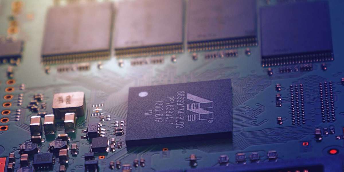
WHAT ARE THE PARTS OF A PCB?
There are a few key parts to any PCB, and understanding each one is essential to creating a successful product. The first part of the PCB is the substrate, or the material on which the electronics will be installed. It's typically a plastic or metal sheet that has been coated with a dielectric material, such as polyester film or aluminum foil. This layer helps insulate the circuitry and prevents it from being damaged by contact with other parts of the PCB.
Next, you'll need to add the layers of circuitry. These can be done in a variety of ways, but common methods include printing circuit boards (PCBs) on silk screen printers or using copper-clad laminate (CCL). CCL is an assembly process where layers of copper have sandwiched a layer of plastic between them. This creates a board that's both flexible and durable.
Once all of the circuitry is installed, you'll need to finish up the PCB by adding protection circuits and connectors. This includes things like e-clip connectors and heat sinks. Heat sinks are particularly important for devices that generate a lot of heat, like digital audio players or laptops.
HOW IS A PCB MANUFACTURED?
A PCB is manufactured by a process called lithography. The image of the circuit or component to be printed is drawn on a thin plastic film (usually less than 0.1 mm thick) using an electronic drawing machine. The film is then cut into small pieces and exposed to a high-pressure jet of chemicals that print the circuit onto the film.
The finished PCBs are then cleaned and dried before they are packaged for shipping.


