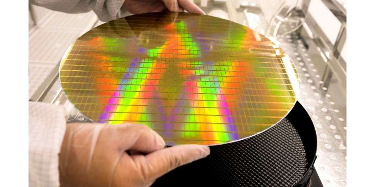
This variation is created by silicon particles and micro-cracks, which provide weak points for metal adhesion. Surface roughness is measured in microns or angstroms, and it varies greatly from the center to the edge of the wafer.
Stylus Profilometer
Stylus profilometers are widely used in the manufacturing industry to determine surface texture. They can measure features as small as one micrometer in height. The measurement principle is simple and straightforward. Stylus profilometers can be easily operated in the production workshop and the metrology lab.
Stylus profilometers operate by moving a small probe over the surface of the wafer. The force that the sample exerts against the probe is measured by a feedback system that keeps the arm at a certain torque. The resulting surface texture is then reconstructed by changing the Z position of the arm holder.
Jupiter
The Jupiter Silicon Wafer Roughness Analyzer is a versatile tool for surface roughness measurements. With its advanced AFM technology, Jupiter delivers measurements with unprecedented speed, precision, and reproducibility. Its modular design allows for multiple configurations and is ideal for high-throughput industrial applications.
Jupiter is capable of measuring angstrom-level roughness of epitaxial silicon layers and heteroepitaxial layers, which are important substrates for high-power microelectronic devices. The software enables flexible location definition and produces images with Rq of 80-85 pm.
Asylum Research
Oxford Instruments recently introduced the Asylum Research Jupiter XR AFM, which leverages Asylum's expertise in developing high-performance AFMs. This new system is designed to provide high-resolution images and reliable, sub-nanometer roughness measurements. It also features high throughput and high measurement confidence.
AFM is a useful tool for studying surface roughness, especially in silicon wafers. Moreover, it also has the ability to measure porosity of low-K materials. However, before using an AFM instrument, users should clarify the type of data they wish to collect. For example, if they only want to compare roughness of similar samples, a regular AFM tip may be enough. However, if they need to compare roughness of samples of different kinds, they may need to use the high resolution tip.
Butterworth high pass filter
The Butterworth high pass filter is one of the most common filters for measuring the roughness of silicon wafers. It has a high pass frequency of about 10 GHz and a low pass frequency of about 1 Hz. Its slope is about 20 dB/decade. This filter is often paired with other filters to form band-pass or band-stop filters.
The Butterworth high pass filter was applied to the global topography data and the spatial cutoff frequency was 440mm. The results showed that the data were similar to the original data, despite the varying surface roughness of the wafer. In addition, it can detect finer surface features. This results in a higher effective roughness value estimated from the height images.
Rigid polishing pads
Rigid silicon wafer polishing pads are designed to remove debris from the front surface of a silicon wafer. During planarization, some of the material is removed from the front surface of the silicon wafer, while some of it remains in the polishing pad. This material can then be rinsed off the pad using deionized water or a slurry.
Rigid silicon wafer polishing pads include an elastic support layer and a polishing layer. These layers are attached to a turn table by double-sided tape. This support layer helps the polishing pad conform to local protrusions in the silicon wafer and reduces the pressure applied to the back surface.
Ethyl silicate
Ethyl silicate is a colloidal silica polishing agent. Its presence in silicon wafer polishing processes improves the surface roughness. The amount of Ethyl Silicate used in silicon polishing processes can be adjusted to produce a smoother surface.
It is also a dopant that improves the mechanical properties of silicon wafers. It helps improve the wettability of photoresist. It is deposited on the wafer surface before deposition of the resist. Silicon wafers can be obtained in an ingot, a circular piece of single-crystal semiconductor material, ready for slicing or shaping into wafers. The ingot undergoes a series of thermal treatments to improve its mechanical and chemical properties. It is then cut into wafers, or sliced, for use in electronics manufacturing.
Acid etching process
Acid etching is a process used to reduce the surface roughness of silicon wafers. However, it can also damage the micro shape of the silicon wafer, and the process is expensive and difficult to control. For this reason, the acid etching process is not suitable for all silicon wafer roughness applications.
The process is generally regarded as effective in minimizing the surface roughness of silicon wafers. Previous studies have shown that the roughness of silicon wafers is highly dependent on the concentration, temperature, and crystallographic orientation. For optical applications, it is important to minimize surface roughness and achieve low light scattering loss.


