If you're looking for a new technology that's making a huge difference in the world, then you've come to the right place. From Integrated circuits and solar cells to nanotechnology research and manufacturing techniques, read on to find out about some of the most fascinating developments.
Integrated circuits
Silicon microelectronics has developed at an exponential rate over the past half century. This has helped to reduce the manufacturing cost of transistors. The technology has also improved functionality, leading to cheaper and high performance electronic devices.
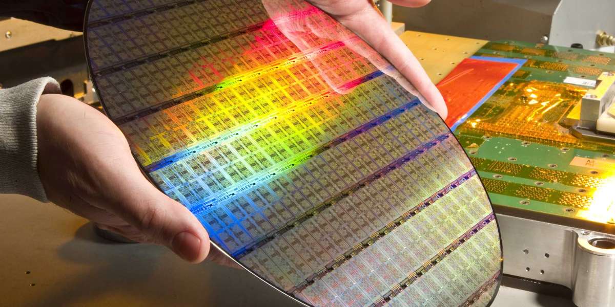
A silicon wafer is a thin slice of monocrystalline silicon. It is used in a wide range of semiconductors. They are often used in nanotechnology research, for example, where they are necessary to carry out complex experiments.
There are two main processes for processing silicon wafers. First, a seed layer is deposited on the surface of the wafer. The thin layer increases the resistivity of the wafer. Typically, the seed layer is a phosphorus-based organic polymer. Second, an ion beam production process is used to create conducting circuitry. This process is able to produce high beam currents, which are essential for connecting people to machines and systems.
Solar cells
Silicon wafers are the best semiconductor material for manufacturing and advanced technological advancements. They are commonly used for manufacture of solar cells, high power LEDs, and computer chips.
In the world of silicon, 300mm silicon wafer segment is widely used for the production of solar cells, LEDs, and other energy-saving gadgets. This segment holds the largest market share in 2021. However, the demand for solar cell technology is increasing globally.
Silicon wafers are the most stable semiconductor materials on the earth. However, they require various microfabrication processes to achieve high-performance solar cells. One of the most significant steps is the texturization process.
The textured surface of a BSi solar cell reduces its reflectance. It also increases the absorption of light. Therefore, it is essential to optimize this process to increase efficiency.
Nanotechnology research
Silicon wafers are used in the manufacturing of semiconductors. They are used in a wide variety of applications, such as consumer electronics, microelectronics, solar cells and medical devices.
There are two primary processes for processing silicon wafers. The first process involves thermal evaporation. This process uses a focused ion beam to evaporate the silicon. It is an expensive process that has several engineering challenges. For example, high power EUV sources can severely heat subsystems in the tool. Consequently, it is important to control temperature to at least 5 mK.
Another process for processing silicon wafers is electron-beam lithography. This method uses a high-pressure gas to emit a beam of light that is then used to trace the die's shape. However, a problem exists with this technique, because it can lead to degradation of costly components.
450-mm silicon wafers
450mm silicon wafers are an important step in the evolution of the semiconductor industry. They are 2.25 times larger than the 300mm diameter wafers currently used. This size is essential to the sustainable development of the semiconductor industry.
The semiconductor industry is driven by Moore's Law, which essentially states that the number of chips produced per wafer increases as the number of silicon wafers decreases. As the silicon wafer size increases, the cost of producing chips reduces.
In order to ensure the long-term sustainability of the semiconductor industry, the industry should adopt precautions to make sure the capital investments made are sustainable. For example, new lithography tools must be developed and implemented by the chip suppliers. These tools will help smooth the transition of the semiconductor industry.
Manufacturing techniques
Silicon wafers are substrates for microelectronic devices. They are used in the creation of integrated circuits, a technology that connects several electronic components together. These devices are used in a wide variety of applications.
Silicon is the most common semiconductor material in the world. It is found in practically all electronic devices. It is also one of the most stable materials. This makes it the ideal substrate for microelectronic devices.
To manufacture silicon wafers, a process is used that combines several process steps. The end result is a smooth, polished surface. There are a variety of different sized wafers, including the standard 200mm and 300mm sizes. Finished wafers have to be sturdy enough to support various applications. A flat zone is applied to the surface to help the device to be oriented properly. Different orient angles are used to determine the depths of dopant penetration and channeling.